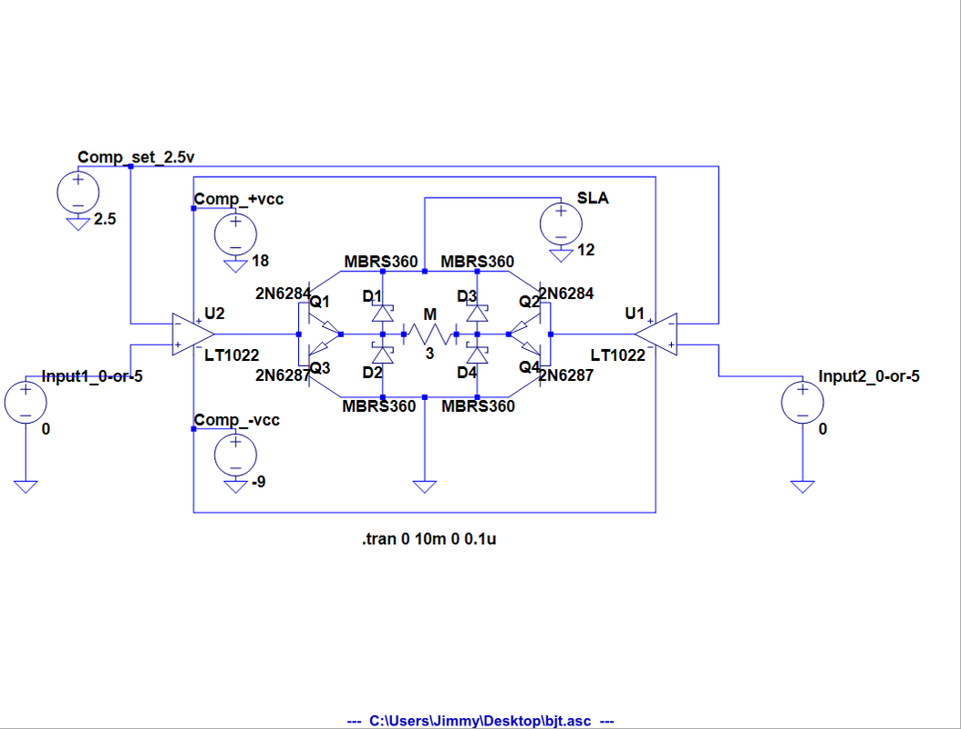
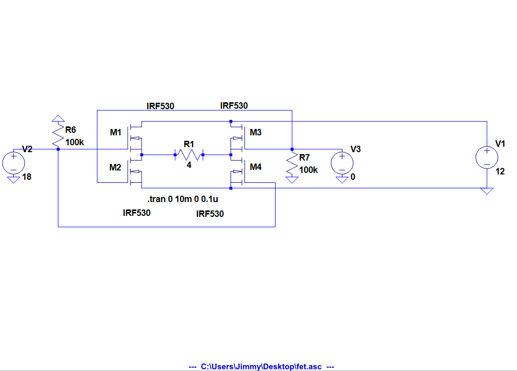
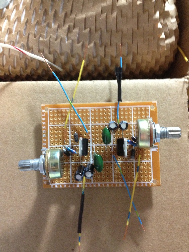
These are some of the H Bridges that I designed with the help from some CAD software during the course of my Design Project.
I initially toyed with the idea of using NPN PNP matched pairs, they worked very well.
I initially toyed with the idea of using NPN PNP matched pairs, they worked very well.
Then I decided that MOSFETs are the way to go (because they don't have the nasty Vce_Sat voltage drop during conduction). Once you reach the threshold voltage it essentially becomes a closed circuit between the drain and source (technically, there is a bit of voltage drop, due to the very minimal Rds_on, usually few tens of milliohms).
Finding matched pairs of high power NMOS and PMOS proved too difficult (we had a budget to keep), so we even tried some designs with just NMOS. But this proved unreliable (due to interference, improper grounding, and lack of a gate resistor), and caused the (catastrophic) destruction of several MOSFETs when the top and bottom MOSFET got turned on simultaneously.
Finding matched pairs of high power NMOS and PMOS proved too difficult (we had a budget to keep), so we even tried some designs with just NMOS. But this proved unreliable (due to interference, improper grounding, and lack of a gate resistor), and caused the (catastrophic) destruction of several MOSFETs when the top and bottom MOSFET got turned on simultaneously.
In the end we went back to the tested and true NPN PNP design and simply raised the base input current using a set of pre-amplifiers using the "ultra reliable" lm395 in between the comparator step and the H bridge.
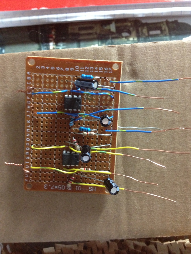
The comparator Op Amps
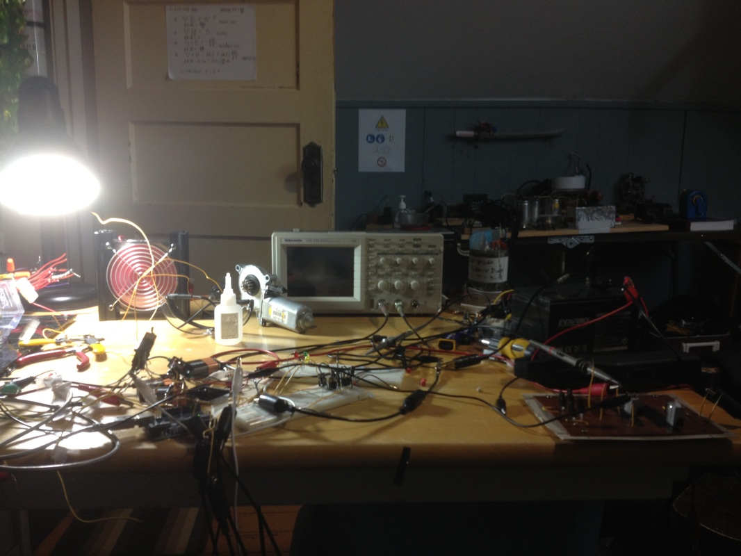
The mess
The LM395 preamp
